How EUVL Chipmaking Works

By: Kevin Bonsor
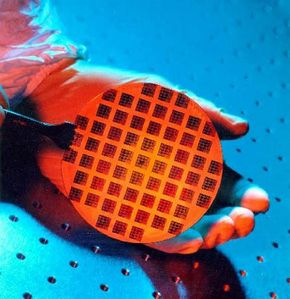
This wafer was patterned on a prototype device using extreme-ultraviolet lithography (EUVL). See more computer hardware pictures.
Photo courtesy Sandia National Laboratories

­Silicon has been the heart of the world's technology boom for nearly half a century, but microprocessor manufacturers have all but squeezed the life out of it. The current technology used to make microprocessors will begin to reach its limit around 2005. At that time, chipmakers will have to look to other technologies to cram more transistors onto silicon to create more powerful chips. Many are already looking at extreme-ultraviolet lithography (EUVL) as a way to extend the life of silicon at least until the end of the decade.

The current process used to pack more and more transistors onto a chip is called deep-ultraviolet lithography, which is a photography-like technique that focuses light through lenses to carve circuit patterns on silicon wafers. Manufacturers are concerned that this technique might soon be problematic as the laws of physics intervene.­

Advertisement

­ Using extreme-ultraviolet (EUV) light to carve transistors in silicon wafers will lead to microprocessors that are up to 100 times faster than today's most powerful chips, and to memory chips with similar increases in storage capacity. In this article, you will learn about the current lithography technique used to make chips, and how EUVL will squeeze even more transistors onto chips beginning around 2007.
Making Chips

Before you learn about how EUV lithography will revolutionize the manufacturing of microprocessors, you should first understand a thing or two about current manufacturing processes. Microprocessors, also called computer chips, are made using a process called lithography. Specifically, deep-ultraviolet lithography is used to make the current breed of microchips and was most likely used to make the chip that is inside your computer.

Lithography is akin to photography in that it uses light to transfer images onto a substrate. In the case of a camera, the substrate is film. Silicon is the traditional substrate used in chipmaking. To create the integrated circuit design that's on a microprocessor, light is directed onto a mask. A mask is like a stencil of the circuit pattern. The light shines through the mask and then through a series of optical lenses that shrink the image down. This small image is then projected onto a silicon, or semiconductor, wafer.

Advertisement

The wafer is covered with a light-sensitive, liquid plastic called photoresist. The mask is placed over the wafer, and when light shines through the mask and hits the silicon wafer, it hardens the photoresist that isn't covered by the mask. The photoresist that is not exposed to light remains somewhat gooey and is chemically washed away, leaving only the hardened photoresist and exposed silicon wafer.

The key to creating more powerful microprocessors is the size of the light's wavelength. The shorter the wavelength, the more transistors can be etched onto the silicon wafer. More transistors equals a more powerful, faster microprocessor. That's the big reason why an Intel Pentium 4 processor, which has 42 million transistors, is faster than the Pentium 3, which has 28 million transistors.

As of 2001, deep-ultraviolet lithography uses a wavelength of 240 nanometers. A nanometer is one-billionth of a meter. As chipmakers reduce to 100-nanometer wavelengths, they will need a new chipmaking technology. The problem posed by using deep-ultraviolet lithography is that as the light's wavelengths get smaller, the light gets absorbed by the glass lenses that are intended to focus it. The result is that the light doesn't make it to the silicon, so no circuit pattern is created on the wafer.

This is where EUVL will take over. In EUVL, glass lenses will be replaced by mirrors to focus light. In the next section, you will learn just how EUVL will be used to produce chips that are at least five times more powerful than the most powerful chips made in 2001.

Moore's Law

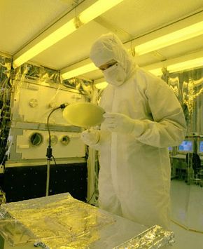
An engineer inspects a wafer freshly printed from the prototype machine using EUVL.
Photo courtesy Sandia National Laboratories

Each year, manufacturers bring out the next great computer chip that boosts computing power and allows our personal computers to do more than we imagined just a decade ago. Intel founder Gordon Moore predicted this technology phenomenon more than 35 years ago, when he said that the number of transistors on a microprocessor would double every 18 months. This became known as Moore's Law.

Industry experts believe that deep-ultraviolet lithography will reach its limits around 2004 and 2005, which means that Moore's law would also come to an end without a new chipmaking technology. But once deep-ultraviolet hits its ceiling, we will see chipmakers move to a new lithography process that will enable them to produce the industry's first 10-gigahertz (GHz) microprocessor by 2007. By comparison, the fastest Intel Pentium 4 processor (as of May 2001) is 2.4 GHz. EUVL could add another 10 years to Moore's Law.

Advertisement

"EUV lithography allows us to make chips with feature sizes that are small enough to support 10 GHz clock speed. It doesn't necessarily make it happen," Don Sweeney, EUV Lithography program manager at Lawrence Livermore National Laboratory (LLNL), said. "The first thing we need to do is to make integrated circuits down to 30 nanometers, and EUV lithography will clearly do that." By comparison, the smallest circuit that can be created by deep-ultraviolet lithography is 100 nanometers.

In April 2001, the EUV Limited Liability Company (EUV LLC) unveiled the first full-scale prototype EUV lithography machine. The EUV LLC is a consortium comprised of some of the world's leading chipmakers and three U.S. Department of Energy research labs. Members include Intel, AMD, IBM, Micron, Infeneon and Motorola. These companies are working with the Virtual National Laboratory, made up of Sandia National Laboratories, Lawrence Livermore National Laboratory and Lawrence Berkeley National Laboratory. The advantage of being a member of this consortium is having first priority to use this new technology.

Now let's see how EUVL works.

The EUVL Process

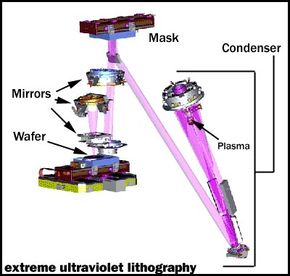
Image source: Sandia National Laboratories

Here's how EUVL works:

  1. A laser is directed at a jet of xenon gas. When the laser hits the xenon gas, it heats the gas up and creates a plasma.
  2. Once the plasma is created, electrons begin to come off of it and it radiates light at 13 nanometers, which is too short for the human eye to see.
  3. The light travels into a condenser, which gathers in the light so that it is directed onto the mask.
  4. A representation of one level of a computer chip is patterned onto a mirror by applying an absorber to some parts of the mirror but not to others. This creates the mask.
  5. The pattern on the mask is reflected onto a series of four to six curved mirrors, reducing the size of the image and focusing the image onto the silicon wafer. Each mirror bends the light slightly to form the image that will be transferred onto the wafer. This is just like how the lenses in your camera bend light to form an image on film.

According to Sweeney, the entire process relies on wavelength. If you make the wavelength short, you get a better image. He says to think in terms of taking a still photo with a camera.

Advertisement

"When you take a photograph of something, the quality of the image depends on a lot of things," he said. "And the first thing it depends on is the wavelength of the light that you're using to make the photograph. The shorter the wavelength, the better the image can be. That's just a law of nature."

As of 2001, microchips being made with deep-ultraviolet lithography are made with 248-nanometer light. As of May 2001, some manufacturers are transitioning over to 193-nanometer light. With EUVL, chips will be made with 13-nanometer light. Based on the law that smaller wavelengths create a better image, 13-nanometer light will increase the quality of the pattern projected onto a silicon wafer, thus improving microprocessor speeds.

This entire process has to take place in a vacuum because these wavelengths of light are so short that even air would absorb them. Additionally, EUVL uses concave and convex mirrors coated with multiple layers of molybdenum and silicon -- this coating can reflect nearly 70 percent of EUV light at a wavelength of 13.4 nanometers. The other 30 percent is absorbed by the mirror. Without the coating, the light would be almost totally absorbed before reaching the wafer. The mirror surfaces have to be nearly perfect; even small defects in coatings can destroy the shape of the optics and distort the printed circuit pattern, causing problems in chip function.

For more information on EUVL and related topics, check out the links on the next page.

Lots More Information