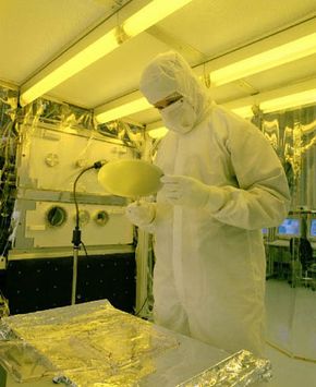
Silicon has been the heart of the world's technology boom for nearly half a century, but microprocessor manufacturers have all but squeezed the life out of it. The current technology used to make microprocessors will begin to reach its limit around 2005. At that time, chipmakers will have to look to other technologies to cram more transistors onto silicon to create more powerful chips. Many are already looking at extreme-ultraviolet lithography (EUVL) as a way to extend the life of silicon at least until the end of the decade.
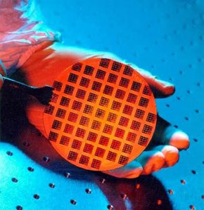
The current process used to pack more and more transistors onto a chip is called deep-ultraviolet lithography, which is a photography-like technique that focuses light through lenses to carve circuit patterns on silicon wafers. Manufacturers are concerned that this technique might soon be problematic as the laws of physics intervene.
Advertisement
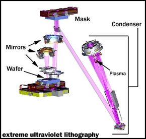
Using extreme-ultraviolet (EUV) light to carve transistors in silicon wafers will lead to microprocessors that are up to 100 times faster than today's most powerful chips, and to memory chips with similar increases in storage capacity. In this article, you will learn about the current lithography technique used to make chips, and how EUVL will squeeze even more transistors onto chips beginning around 2007.