How small can CPUs get?

By: Jonathan Strickland  | 
Gordon Moore
Intel co-founder Gordon Moore made the original observation that evolved into Moore's Law. See more computer hardware pictures.
Justin Sullivan/Getty Images

­During the 20th century, inventors created devices that the public regularly depended upon. Arguably, one of the most important inventions was the transistor. Developed in 1947 by engineers working for Bell Laboratories, the original purpose of the transistor was to amplify sound over phone lines. The transistor replaced an older technology — vacuum tubes. The tubes weren't reliable, were bulky and generated a lot of heat, too.

The first transistor was a point-contact transistor that measured half an inch (1.27 centimeters) in height. The transistor wasn't very powerful, but physicists recognized the potential of the device. Before long, physicists and engineers began to incorporate transistors into various electronic devices. And as time passed, they also learned how to make transistors smaller and more efficient.

Advertisement

In 1958, engineers attached two transistors to a silicon crystal and created the world's first integrated circuit [source: Intel]. In turn, the integrated circuit paved the way for the development of the microprocessor. If you compare a computer to a human being, the microprocessor would be the brain. It makes calculations and processes data.

By the 1960s, computer scientist (and Intel co-founder) Gordon Moore made an interesting observation: He noticed that every 12 months, engineers were able to double the number of transistors on a square-inch piece of silicon. Like clockwork, engineers were finding ways to reduce the size of transistors. It's because of these small transistors that we have electronic devices like personal computers, smartphones and mp3 players. Without transistors, we would still be using vacuum tubes and mechanical switches to make calculations.

­Since Moore's observation, the shrinking trend has continued. But it hasn't kept up with the pace Moore observed. These days, the number of transistors doubles every 24 months. But that raises an interesting question: How small can transistors — and by extension, CPUs — get? In 1947, a single transistor measured a little over one-hundredth of a meter high. By the 2010s, Intel produced microprocessors with transistors measuring only 45 nanometers wide. A nanometer is one-billionth of a meter!

Intel and other microprocessor manufacturers are already working on the next generation of chips. These will use transistors measuring a mere 32 nanometers in width. But some physicists and engineers think we might be bumping up against some fundamental physical limits when it comes to transistor size.

Advertisement

Anatomy of a Transistor

Xeon Processor
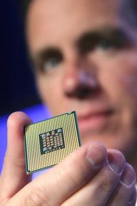
Intel vice president Tom Kilroy holds a Dual-Core Xeon Processor 5100 at a press event in San Francisco.
Court Mast/Intel via Getty Images

Before we go into the physical limitations of transistors, it helps to know what a transistor consists of and what it actually does. Basically, a transistor is a switch made out of a special kind of matter. One way you can classify matter is by looking at how well it can conduct electricity. That divides matter into three categories: conductors, insulators and semiconductors. A conductor is any type of material made of atoms with free spaces for electrons. An electric current can pass through conductive material — metals tend to be good conductors. An insulator is matter composed of atoms that don't have any electron spaces available. As a result, electricity can't flow through these materials. Ceramic or glass are good examples of insulators.

Semiconductors are a bit different. They are composed of matter with atoms that have some space for electrons but not enough to conduct electricity the way metals do. Silicon is such a material. Under some circumstances, silicon can act as a conductor. Under others, it acts as an insulator. By tweaking these circumstances, it's possible to control the flow of electrons. This simple concept is the foundation for the most advanced electronic devices in the world.

Advertisement

Engineers discovered that by doping — introducing certain kinds of material — into silicon, they could control its conductivity. They'd start with a base called a substrate and dope it with either negatively charged or positively charged material. Negatively charged material has an excess of electrons while positively charged material has an excess of holes — places where electrons could fit. In our example, we'll consider an n-type transistor, which has a positively charged substrate.

­On this foundation are three terminals: a source, a drain and a gate. The gate sits between the source and the drain. It acts as a door through which voltage can pass into the silicon but not back out. The gate has a thin layer of insulator called an oxide layer that prevents electrons from passing back through the terminal. In our example, the insulator is between the gate and the positively charged substrate.

The source and drain in our example are negatively charged terminals. When you apply a positive voltage to the gate, it attracts the few free electrons in the positively charged substrate to the gate's oxide layer. This creates an electron channel between the source and drain terminals. If you then apply a positive voltage to the drain, electrons will flow from the source through the electron channel to the drain. If you remove the voltage from the gate, the electrons in the substrate are no longer attracted to the gate and the channel is broken. That means when you've got a charge to the gate, the transistor is switched to "on." When the voltage is gone, the transistor is "off."

Electronics interpret this switching as information in the form of bits and bytes. That's how your computer and other electronic devices process data. But because electronics depend on the movement of electrons to process information, they're subject to some special laws of physics. We'll take a closer look into them in the next section.

Advertisement

Transistors on the Nanoscale

Pentium 4 processors
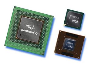
The Pentium 4 processor family.
Intel/Newsmakers via Getty Images

It seems like every year a journalist publishes an article that says transistors are as small as they'll ever get and Moore's Law is no more. Then engineers find innovative ways to create even smaller transistors and prove the journalist wrong. We've reached a point where many writers are gun-shy when it comes to predicting the end of Moore's Law.

But it's true that one day we'll hit the physical limits of how small traditional transistors can be. That's because once you hit the nanoscale, you're dealing with the bizarre world of quantum mechanics. In this world, matter and energy behave in ways that seem counterintuitive. Quantum physics is very different from classic physics — you can't even observe something on the quantum scale without affecting its behavior.

Advertisement

One quantum effect is electron tunneling, which is a bit like teleportation. When material is very thin — the thickness of a single nanometer (about 10 atoms thick) — electrons can tunnel right through it as if it weren't there at all. The electron doesn't actually make a hole through the material. Instead, the electron disappears from one side of the barrier and reappears on the other. Since gates are meant to control the flow of electrons, this is a problem. If electrons can pass through a gate under any set of circumstances, there's no way to control their flow. With leaky transistors, the flow of electrons can't be controlled, so the processor would be ineffective or not functional at all.

With companies like Intel working on transistors that measure only 32 nanometers in width, it won't be long before the oxide layer becomes too thin to act as a gate for electrons ­using traditional transistors. While engineers have hit some obstacles during the race to shrink transistors in the past, they've always found some way to work around the problem and keep up with Moore's Law. But those days could end once we face a fundamental law of physics.

It's possible that engineers will discover a way to create an effective insulator even at a thickness of one nanometer. But even if they manage to do that, there's not much further they can go with transistors as we know them today. After all, beyond the nanoscale is the atomic scale, where you're dealing with materials that are only a few atoms in size.

This doesn't mean that transistors will go away. But it might mean that the advancements in microprocessor development will slow down and level off. Improvements in processing power may not continue to be exponential. But companies will likely find ways to improve microprocessor efficiency and performance, nonetheless.

There's also the possibility that microprocessor manufacturers will find an alternative to transistors. And some are already looking into ways to harness the quantum effects of the nanoscale — effectively turning nano-lemons into nano-lemonade.

It seems like microprocessor manufacturers will only be able to keep Moore's Law going for a few more years. But if you look back at the predictions from decades ago, you'll see journalists making that same claim. Maybe engineers see these predictions as a personal challenge to find ways around seemingly insurmountable obstacles.

Advertisement

Lots More Information

Related How Stuff Works Articles

More Great Links

  • Broad, William J. "Incredible Shrinking Transistor Nears Its Ultimate Limit: The Laws of Physics." The New York Times. Feb. 4, 1997. (Dec. 17, 2008) http://query.nytimes.com/gst/fullpage.html?res=9D05E3DB113DF937A35751C0A961958260
  • Devoret, Michel and Glattli, Christian. "Single-electron transistors." Physics World. Sept. 1, 1998. (Dec. 18, 2008)
  • Engel, Justin. "Are transistors on the way out?" MLive.com. Dec. 19, 2007. (Dec. 18, 2008)
  • Flatow, Ira. "Transistorized!" PBS. 1999. (Dec. 18, 2008) http://www.pbs.org/transistor/index.html
  • Föll, Helmut "General Aspects of Silicon Technology." University of Kiel, Faculty of Engineering. (Dec. 17, 2008) http://www.tf.uni-kiel.de/matwis/amat/elmat_en/kap_5/backbone/r5_0_1.html
  • Intel. "Architecture & Silicon Technology." (Dec. 17, 2008) http://www.intel.com/technology/architecture-silicon/index.htm?iid=tech_home+body_ architecturesilicon
  • Kelsall, Robert et al. "Nanoscale Science and Technology." John Wiley & Sons, Ltd. 2005.
  • Levi, A. F. J. "Applied Quantum Mechanics." Cambridge University Press. Cambridge, UK. 2003.
  • Science Daily. "Pushing the Limits of Computer Chip Miniaturization." Jan. 14, 2008. (Dec. 18, 2008) http://www.sciencedaily.com/releases/2008/01/080112083626.htm

Advertisement

Loading...