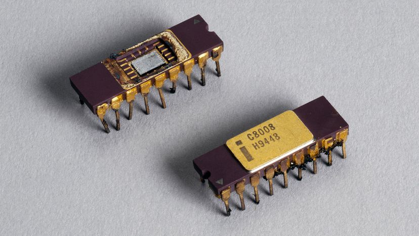
Even the incredibly simple microprocessor shown in the previous example has a fairly large set of instructions that it can perform. The collection of instructions is implemented as bit patterns, each one of which has a different meaning when loaded into the instruction register. Humans are not particularly good at remembering bit patterns, so a set of short words are defined to represent the different bit patterns. This collection of words is called the assembly language of the processor. An assembler can translate the words into their bit patterns very easily, and then the output of the assembler is placed in memory for the microprocessor to execute.
Here's the set of assembly language instructions that the designer might create for the simple microprocessor in our example:
- LOADA mem - Load register A from memory address
- LOADB mem - Load register B from memory address
- CONB con - Load a constant value into register B
- SAVEB mem - Save register B to memory address
- SAVEC mem - Save register C to memory address
- ADD - Add A and B and store the result in C
- SUB - Subtract A and B and store the result in C
- MUL - Multiply A and B and store the result in C
- DIV - Divide A and B and store the result in C
- COM - Compare A and B and store the result in test
- JUMP addr - Jump to an address
- JEQ addr - Jump, if equal, to address
- JNEQ addr - Jump, if not equal, to address
- JG addr - Jump, if greater than, to address
- JGE addr - Jump, if greater than or equal, to address
- JL addr - Jump, if less than, to address
- JLE addr - Jump, if less than or equal, to address
- STOP - Stop execution
If you have read How C Programming Works, then you know that this simple piece of C code will calculate the factorial of 5 (where the factorial of 5 = 5! = 5 * 4 * 3 * 2 * 1 = 120):
a=1;f=1;while (a <= 5){ f = f * a; a = a + 1;}
At the end of the program's execution, the variable f contains the factorial of 5.
Assembly Language
A C compiler translates this C code into assembly language. Assuming that RAM starts at address 128 in this processor, and ROM (which contains the assembly language program) starts at address 0, then for our simple microprocessor the assembly language might look like this:
// Assume a is at address 128// Assume F is at address 1290 CONB 1 // a=1;1 SAVEB 1282 CONB 1 // f=1;3 SAVEB 1294 LOADA 128 // if a > 5 the jump to 175 CONB 56 COM7 JG 178 LOADA 129 // f=f*a;9 LOADB 12810 MUL11 SAVEC 12912 LOADA 128 // a=a+1;13 CONB 114 ADD15 SAVEC 12816 JUMP 4 // loop back to if17 STOP
ROM
So now the question is, "How do all of these instructions look in ROM?" Each of these assembly language instructions must be represented by a binary number. For the sake of simplicity, let's assume each assembly language instruction is given a unique number, like this:
- LOADA - 1
- LOADB - 2
- CONB - 3
- SAVEB - 4
- SAVEC mem - 5
- ADD - 6
- SUB - 7
- MUL - 8
- DIV - 9
- COM - 10
- JUMP addr - 11
- JEQ addr - 12
- JNEQ addr - 13
- JG addr - 14
- JGE addr - 15
- JL addr - 16
- JLE addr - 17
- STOP - 18
The numbers are known as opcodes. In ROM, our little program would look like this:
// Assume a is at address 128// Assume F is at address 129Addr opcode/value0 3 // CONB 11 12 4 // SAVEB 1283 1284 3 // CONB 15 16 4 // SAVEB 1297 1298 1 // LOADA 1289 12810 3 // CONB 511 512 10 // COM13 14 // JG 1714 3115 1 // LOADA 12916 12917 2 // LOADB 12818 12819 8 // MUL20 5 // SAVEC 12921 12922 1 // LOADA 12823 12824 3 // CONB 125 126 6 // ADD27 5 // SAVEC 12828 12829 11 // JUMP 430 831 18 // STOP
You can see that seven lines of C code became 18 lines of assembly language, and that became 32 bytes in ROM.
Decoding
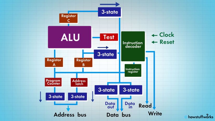
The instruction decoder needs to turn each of the opcodes into a set of signals that drive the different components inside the microprocessor. Let's take the ADD instruction as an example and look at what it needs to do:
- During the first clock cycle, we need to load the instruction. Therefore, the instruction decoder needs to:
- activate the tri-state buffer for the program counter
- activate the RD line
- activate the data-in tri-state buffer
- latch the instruction into the instruction register
- During the second clock cycle, the ADD instruction is decoded. It needs to do very little:
- set the operation of the ALU to addition
- latch the output of the ALU into the C register
- During the third clock cycle, the program counter is incremented (in theory this could be overlapped into the second clock cycle).
Every instruction can be broken down as a set of sequenced operations like these that manipulate the components of the microprocessor in the proper order. Some instructions, like this ADD instruction, might take two or three clock cycles. Others might take five or six clock cycles.